India's Semiconductor Manufacturing Push: Which Parts of the Supply Chain Offer the Biggest Opportunities?
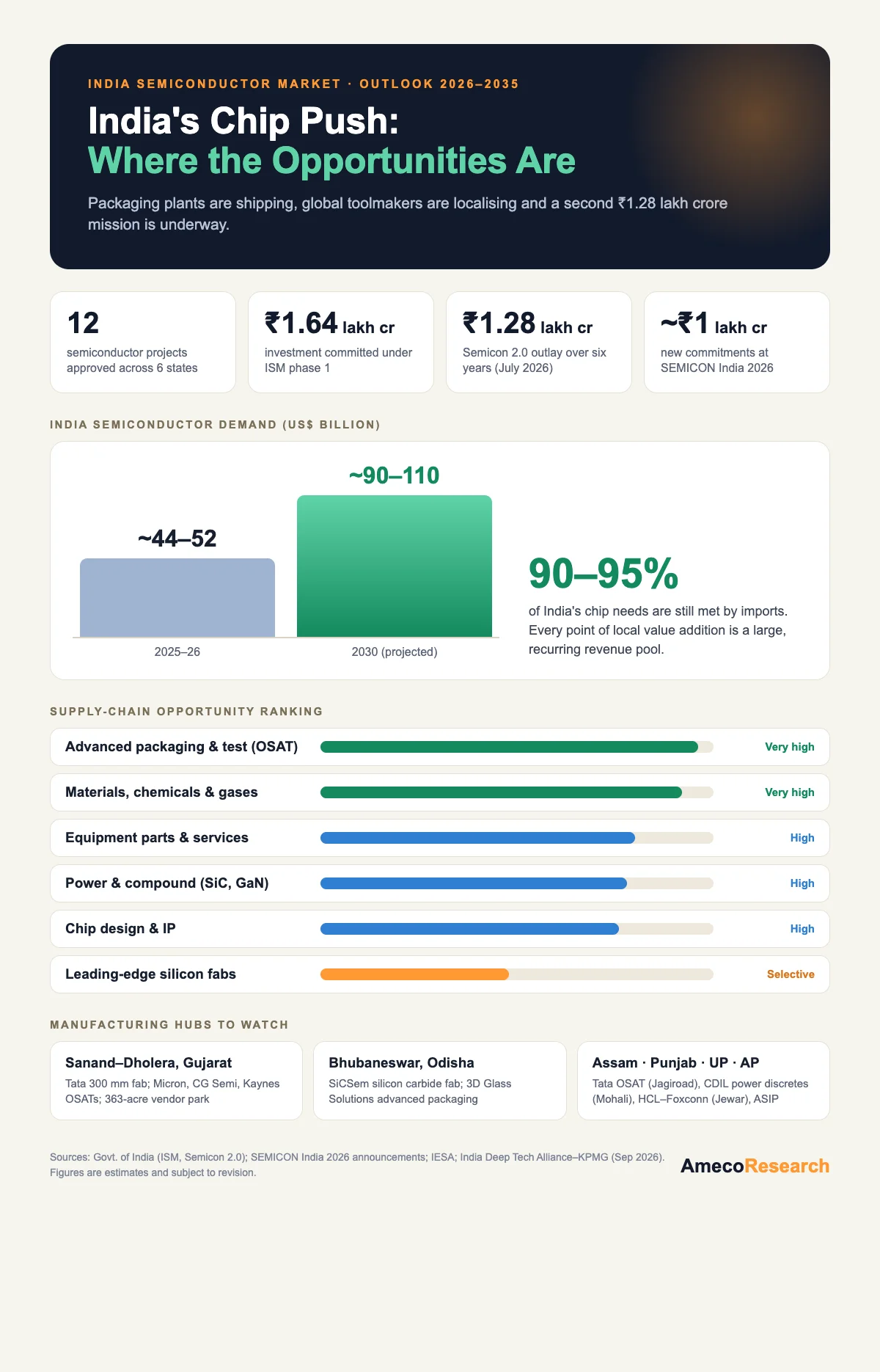
Quick answer: India's semiconductor push has moved from policy to production. Twelve projects worth more than ₹1.64 lakh crore are approved, the first packaging plants are shipping commercial chips, and the government has added a second, ₹1.28 lakh crore phase of the India Semiconductor Mission. The biggest near-term opportunities sit in advanced packaging and testing (OSAT), fab-grade materials, chemicals and gases, equipment parts and services, and power and compound semiconductors, where demand is visible and India's import dependence is highest.
Key Takeaways
- Projects: 12 semiconductor manufacturing projects approved across six states, with investment commitments above ₹1.64 lakh crore. They include one silicon fab, one silicon carbide fab, a gallium nitride micro-LED display fab and nine packaging units.
- Production has started: Micron, CG Semi and Kaynes Semicon are in commercial production, and SEMICON India 2026 saw new lines open at Suchi Semicon in Surat and CDIL in Mohali.
- More money is coming: the Cabinet approved Semicon 2.0 on 15 July 2026 with an outlay of about ₹1.28 lakh crore over six years, covering design, equipment, materials, chemicals, gases, fabs, packaging, R&D and talent.
- Demand is large and mostly imported: India's chip consumption is estimated at roughly US$45–52 billion today and is projected to reach about US$90–110 billion by 2030, while an estimated 90–95% of requirements are met through imports.
- The supply base is arriving: Applied Materials, Lam Research, Tokyo Electron, Fujifilm, JSR and others announced India plans at SEMICON India 2026.
Why 2026 Is a Turning Point for the India Semiconductor Market
For most of the last decade, India's chip story was about intent. That changed in 2026. The first ISM-backed assembly and test plants began shipping commercial devices, global equipment makers committed real capital, and the government doubled down with a second, larger incentive programme.
SEMICON India 2026, held at Yashobhoomi in New Delhi from 17 to 19 September, showed how far things have moved. More than 600 companies from 52 countries took part, and the opening day alone produced investment commitments of about ₹1 lakh crore, which officials expect to create close to one lakh jobs over the next two to three years.
Where India Stands: The Approved Project Scorecard
The table below summarises the major projects approved under the first phase of the India Semiconductor Mission and their status as of October 2026.
| Project | Location | Type | Status |
|---|---|---|---|
| Tata Electronics with PSMC | Dholera, Gujarat | 300 mm silicon fab (28–110 nm), about 50,000 wafer starts a month | Under construction |
| Micron Technology | Sanand, Gujarat | Memory assembly and test (DRAM, NAND) | Commercial production |
| Tata Semiconductor Assembly and Test | Jagiroad, Assam | Large-scale OSAT | Under construction |
| CG Semi (with Renesas and Stars Microelectronics) | Sanand, Gujarat | OSAT | Commercial production |
| Kaynes Semicon | Sanand, Gujarat | OSAT | Commercial production |
| HCL–Foxconn joint venture | Jewar, Uttar Pradesh | OSAT for display driver chips | Under construction |
| SiCSem (with Clas-SiC) | Bhubaneswar, Odisha | Silicon carbide compound fab and packaging | Under construction |
| 3D Glass Solutions | Bhubaneswar, Odisha | Glass-substrate advanced packaging | Under construction |
| CDIL | Mohali, Punjab | Power discretes in silicon and silicon carbide | Line inaugurated, September 2026 |
| ASIP Technologies (with APACT) | Andhra Pradesh | OSAT | Under construction |
Two patterns stand out. First, back-end assembly and test is ahead of front-end fabrication; every plant shipping commercial product today is a packaging or test unit. Second, the projects cluster in a handful of hubs, led by Gujarat's Sanand–Dholera corridor and Odisha's Info Valley, which concentrates supplier demand in places where local capacity is still thin.
The Opportunity Map: Ranking the Semiconductor Supply Chain
Not every segment offers the same mix of demand, timing and policy support. Here is how we rank the main parts of the chain for investors and suppliers looking at India over 2026–2035.
| Segment | Opportunity | Why |
|---|---|---|
| Advanced packaging and test (OSAT) | Very high | Most mature segment, plants already shipping, higher 35% support for advanced packaging |
| Materials, chemicals and gases | Very high | Every fab and OSAT needs local supply; explicitly covered by Semicon 2.0 |
| Equipment parts and services | High | Global toolmakers localising parts, components and service networks |
| Power and compound semiconductors | High | EV, renewables and grid demand; SiC fab and power discrete lines approved |
| Chip design and IP | High | India's deepest talent pool; Semicon 2.0 targets 200 design start-ups |
| Leading-edge silicon fabs | Selective | Long gestation and very high capital needs; first fab still under construction |
1. Advanced Packaging, Assembly and Testing
Packaging is where India is winning first. Assembly, test, marking and packaging (ATMP) plants need less capital than fabs, ramp faster and can serve global customers from day one. Five back-end units are already in commercial production, and officials say Indian ATMP output is being shipped to Japan and built into products exported to the US and Europe.
The next wave is more advanced. Semicon 2.0 offers higher support for advanced packaging than for legacy packaging, and approved projects now include glass substrates and 3D heterogeneous integration in Odisha.
Where suppliers fit: substrates, lead frames, bonding wire, encapsulants, die-attach materials, test sockets, burn-in boards and test services. Related reading: our Hermetic Packaging Market report and Thermal Interface Materials Market report.
2. Materials, Specialty Chemicals and Gases
A fab consumes hundreds of ultra-pure inputs: photoresists, wet chemicals, CMP slurries, specialty and bulk gases, sputtering targets, and silicon wafers. Almost none of these are made in India at semiconductor grade today, which makes this the clearest import-substitution opportunity in the chain.
Movement is visible. Tata Electronics signed agreements with Fujifilm and JSR on localising critical materials and advanced chemicals, and with Sumitomo Chemical and INOX Air Products on chemicals and gases. It is also developing a 363-acre vendor park at Dholera so suppliers can locate next to the fab. Semicon 2.0 explicitly extends incentives to makers of chemicals, gases and materials for the first time.
Where suppliers fit: electronic-grade chemicals, high-purity gases and gas delivery systems, wafer handling consumables and cleanroom supplies. See our Specialty Chemicals Market report.
3. Semiconductor Equipment, Parts and Services
The near-term opportunity is in the components, sub-assemblies, refurbishment, installation and field service that toolmakers need close to their customers.
SEMICON India 2026 delivered the strongest signal yet. Applied Materials announced its "India Vision 2035," a US$5 billion plan over the decade that includes a 10x expansion of its India supply chain capacity and a 140-acre research park. Lam Research announced about ₹10,000 crore for its first silicon component manufacturing facility in India, covering processing from silicon ingot onward and serving as an export base.
Where suppliers fit: precision-machined parts, vacuum and fluid components, RF and power sub-systems, chamber parts, cleaning and coating services, and trained field engineers.
4. Power Electronics and Compound Semiconductors
Electric vehicles, solar inverters, data centres and grid upgrades all depend on power devices.
SiCSem's silicon carbide facility in Bhubaneswar is planned as India's first commercial compound semiconductor fab, with capacity for 60,000 wafers a year. CDIL's Mohali expansion covers MOSFETs, IGBTs and Schottky diodes in both silicon and silicon carbide. At SEMICON India 2026, Tata Electronics and Nexperia agreed to work on MOSFET production at Dholera and assembly and test of discrete products in Assam.
Where suppliers fit: SiC and GaN substrates and epitaxy, power modules, gate drivers and thermal management. Related reading: our Insulated Gate Bipolar Transistor Market report and Electric Vehicle Market report.
5. Chip Design, IP and Talent
Design remains India's strongest card. Under the Design Linked Incentive scheme, 24 design projects have received support and 105 start-ups and MSMEs have access to industry-standard EDA tools. Of those, about 20 have raised venture capital, and the government's new target is 200 design start-ups.
Talent programmes are scaling in parallel. About 70,000 design engineers have been trained in four years, Lam Research aims to train up to 60,000 students through its virtual fab platform, and Semicon 2.0 proposes training one lakh technicians over five years. See our Radio Frequency Semiconductor Market report for one of the design-heavy segments where Indian teams are active.
6. Silicon Fabrication
Front-end fabrication is the anchor that pulls every other segment along, but it is also the slowest and most capital-hungry. Tata Electronics' Dholera fab, designed for 28 nm and more mature nodes, is still under construction, with the company putting its combined investment at about US$14 billion. Semicon 2.0 supports 40% of eligible capital cost for silicon fabs and 35% for compound semiconductor, sensor and display fabs, and funds R&D toward nodes beyond today's 28–110 nm range.
Demand Outlook: How Big Is the India Semiconductor Market?
India's semiconductor consumption is already substantial. The India Electronics and Semiconductor Association put it at about US$52 billion in 2024–25 and projects around US$103 billion by 2030. A September 2026 study by the India Deep Tech Alliance and KPMG in India estimates demand rising from about US$44 billion in 2025–26 to about US$90 billion by 2029–30.
Mobile devices and wearables are the largest end market, followed by telecom, IT and industrial electronics, with automotive and defence growing fastest from a smaller base. For the global picture, see our Semiconductor Market report.
The key point for 2026–2035 is the gap between demand and local supply. With imports of integrated circuits alone exceeding US$30 billion in 2025–26, every percentage point of local value addition represents a large and recurring revenue pool.
Risks Investors Should Price In
- Commitments are not spending: much of the ₹1 lakh crore announced at SEMICON India 2026 still needs board approvals and will be deployed over two to three years.
- Fab execution: India's first commercial wafer fab is not yet producing, and delays would push back demand for materials and services.
- Utilities: fabs need reliable power and very large volumes of ultra-pure water; hub infrastructure is still being built.
- Talent depth: India has strong design talent but limited experience in fab operations and process engineering.
Our Outlook for 2026–2035
India's semiconductor build-out will be won from the back end forward. Packaging, testing, materials and equipment services are where demand is already real and where policy support is strongest. Power and compound semiconductors offer a differentiated path tied to electric vehicles and the energy transition. Design will keep compounding India's existing advantage.
The indicators worth tracking are first wafer output at Dholera, utilisation at the operating OSAT plants, the number of supplier units in the Dholera vendor park, and how quickly Semicon 2.0 incentives flow to materials and equipment makers. Contact Ameco Research for a customised India semiconductor market study covering segment sizing, supplier mapping and entry strategy.
Frequently Asked Questions
How big is the India semiconductor market?
India's semiconductor consumption is estimated at roughly US$45–52 billion today and is projected to reach about US$90–110 billion by 2030, driven by smartphones, telecom, IT hardware, industrial electronics and automotive.
What is Semicon 2.0 (India Semiconductor Mission 2.0)?
Semicon 2.0 is the second phase of the India Semiconductor Mission, approved on 15 July 2026 with an outlay of about ₹1.28 lakh crore over six years. It covers chip design, equipment, materials, chemicals, gases, fabs, advanced packaging, R&D and talent.
How many semiconductor projects has India approved?
India has approved 12 semiconductor manufacturing projects across six states with investment commitments above ₹1.64 lakh crore, including one silicon fab, one silicon carbide fab, a gallium nitride micro-LED display fab and nine packaging units.
Which semiconductor plants in India are in production?
Micron, CG Semi and Kaynes Semicon are in commercial production, and new lines at Suchi Semicon in Surat and CDIL in Mohali opened during SEMICON India 2026. All plants in production are assembly, test or packaging units; the first commercial wafer fab at Dholera is under construction.
Which part of the semiconductor supply chain offers the biggest opportunity in India?
Advanced packaging and testing, along with semiconductor-grade materials, chemicals and gases, offer the biggest near-term opportunities because plants are already operating and nearly all inputs are currently imported. Equipment parts and services, power semiconductors and chip design are close behind.
Sources: Government of India and Cabinet releases on the India Semiconductor Mission and Semicon 2.0; SEMICON India 2026 coverage by The Tribune and EE Times; company announcements by Applied Materials, Lam Research and Tata Electronics; India Electronics and Semiconductor Association; India Deep Tech Alliance and KPMG in India (September 2026). Figures are estimates and may be revised. This article is for information only and is not investment advice.